The atomic-scale confinement of the self-assembled photonic cavities
Anomalous diffraction field enhancement in a single silicon bowtie: from nanofabrication to self-assembly
Because miniaturization is required for realizing bowtie cavities5 with ultra small mode volumes, it’s been added to the centre stage in photonics. Part of the reason that realistic designs were missing and that experimental progress was impeded was due to the fact that there weren’t many designs for the dyneiwode with mode volumes below the limit. The field discontinuities at the material boundaries hold the promise of unprecedented light–matter interaction strengths, fostering new developments in nanolasers and optical interconnects. The field enhancement22 is determined by the width of the bowtie. Although little can be done to change the course of conventional lithography or etching to atomic dimensions, the first experiment was able to show that confinement of light below the diffraction limit in the dielectric bowtie can be accomplished with 8 NIT wide Silicon bridges with 30 aspect ratios. Void or low-refractive-index features with extreme aspect ratios are especially challenging to fabricate, but they are required for some of the most radical applications of nanocavities, such as bulk non-linearities operating at the single-photon level25 and single-photon emitters for quantum photonic integrated circuits28. While top-down nanofabrication in modern foundry production allows defining the position of edges with both precision and accuracy (disorder) at the level of a single silicon atom29, the resolution limit (the smallest possible linewidth) of approximately 50 atoms has so far hindered such developments, see Supplementary Information Section 1.
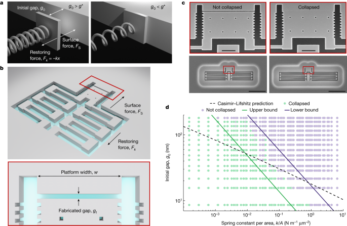
Here we propose and demonstrate a new approach to the manufacturing of semiconductor devices. The Casimir-van der Waals force 4,30 is one example of the surface forces that can be used to make devices with unprecedented dimensions. Our experiments harness the forces that cause the failure of micro- and nanomechanical devices to enable controlled collapses to fabricate smaller, more intricate structures.
The fabrication of functional materials and devices at the micro- and nanoscale typically follows either a top-down approach based on planar technology or a bottom-up approach, where structures are self-assembled using various effects, such as van der Waals, electrostatic, capillary or hydrogen-bonding forces8,9,10,11,12. The bottom-up approach has enabled a lot of research on devices with near-atomic dimensions. A wealth of research and technology depends on a higher surface to volume ratio, strong field gradients or quantum effects for miniaturization. However, the miniaturization of semiconductor technology has slowed, and the current industry roadmap forecasts no lateral lithography features (minimum half-pitch or physical gate length) below 8 nm until 2037. At the same time, while bottom-up approaches can achieve feature sizes down to atomic scales, synthetic self-assembly remains far from capable of replicating the hierarchical and scalable self-assembly in biological systems13. A practical consequence is that a wealth of research on bottom-up nanotechnology for information technology always had to rely on top-down technology for the interconnect architecture. If you want to contact a singlemolecule device, you must use wires or waveguides. The vast views of top- down technology with the resolution of bottom up approaches are commonly considered disjoint. Microelectromechanical systems can be fabricated using self-assembly, but not with their nanoscale dimensions. The pathway for direct integration of self-assembly and technology is hard to find.